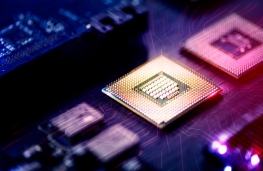
Information and Communication
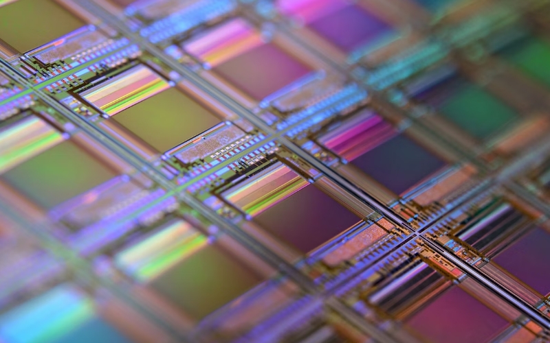
This is the core field, encompassing all devices that process and transmit information, such as computers, mobile phones, data centers, and communication networks.
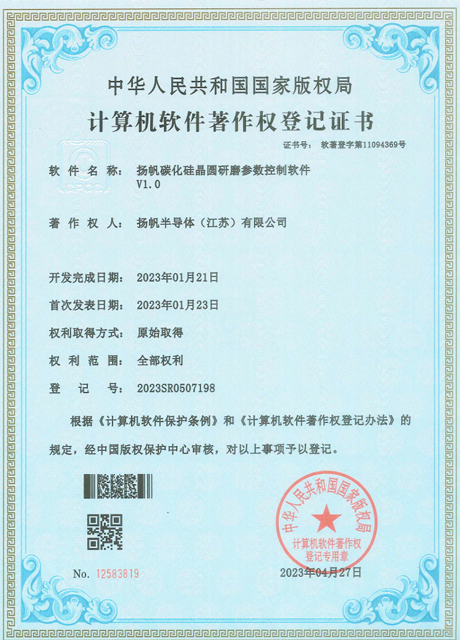
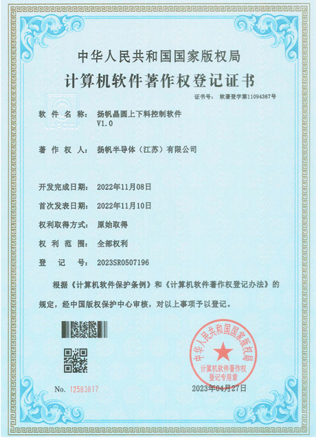
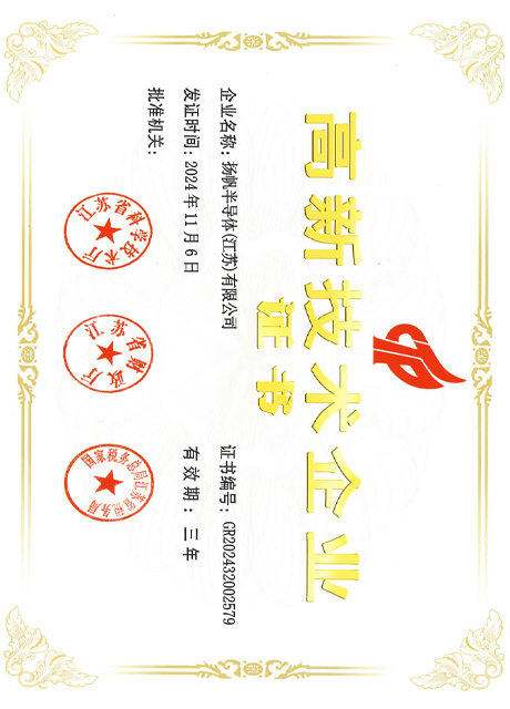
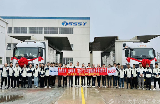
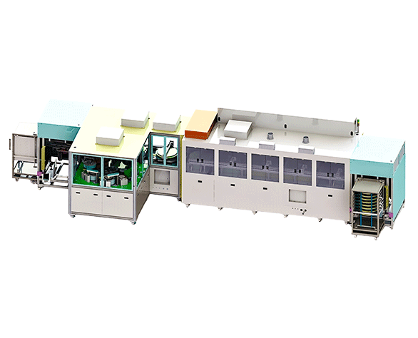
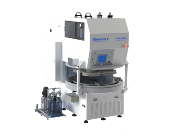
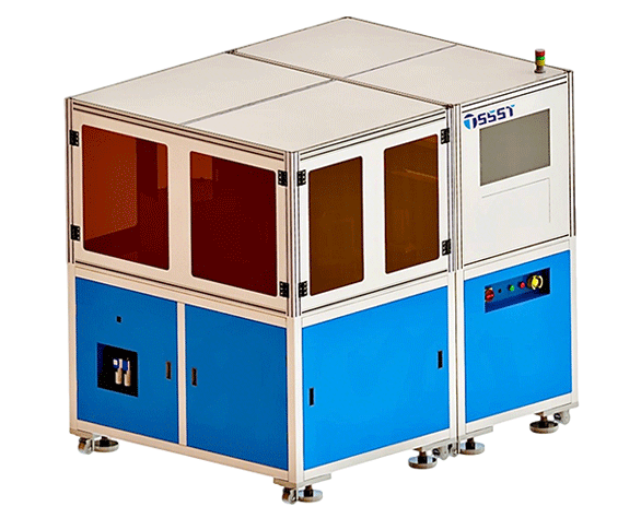
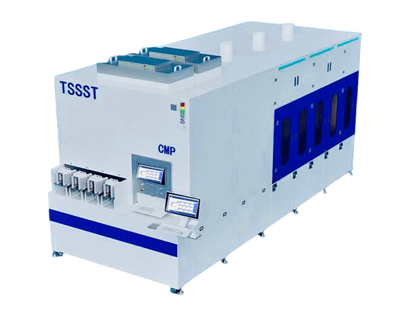
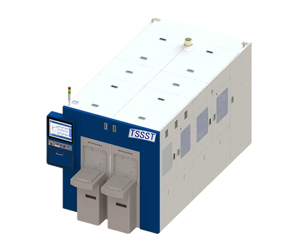
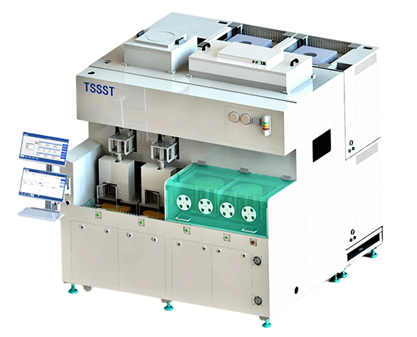
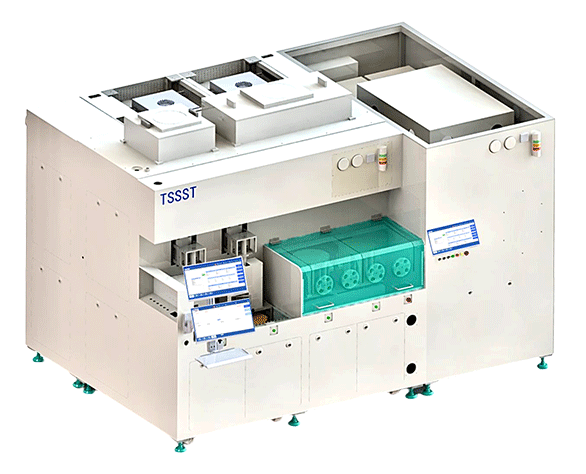
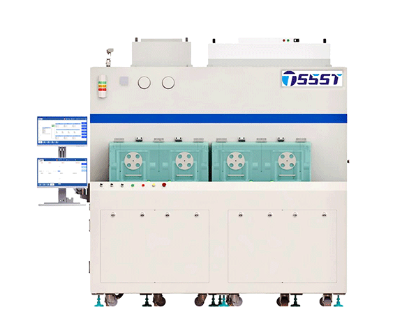
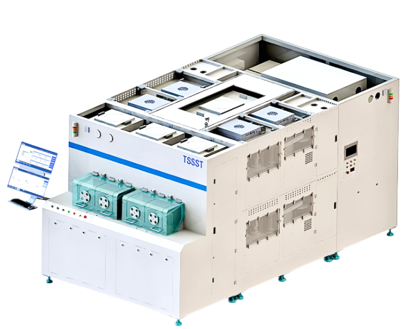
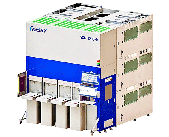
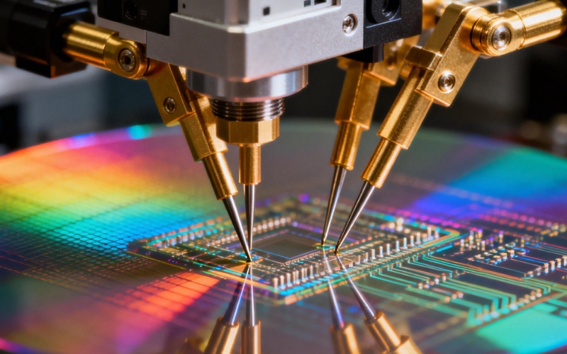
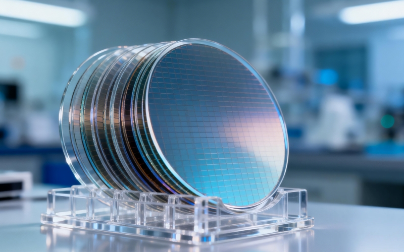
Yangfan Semiconductor (Jiangsu) Co., Ltd. has an equipment subsidiary founded in 2018, a high-tech enterprise specializing in the R&D, manufacturing and sales of semiconductor equipment, driving the upgrading of the global semiconductor industry through technological innovation. Located at No. 58 Meiyan West Road, Pingwang Town, Wujiang District, Suzhou City, the company lies in the core area of the Yangtze River Delta semiconductor industry cluster. It covers an area of 37 mu with a building area of 11,331 square meters, providing solid support for production and R&D.
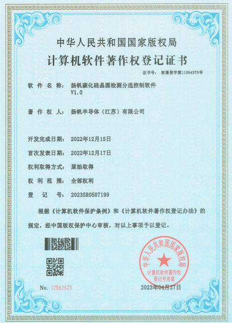
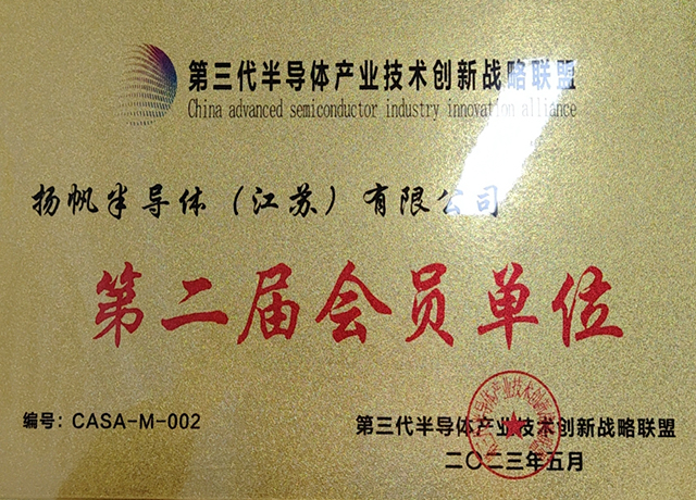
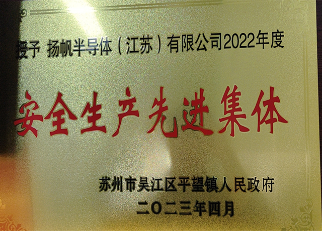
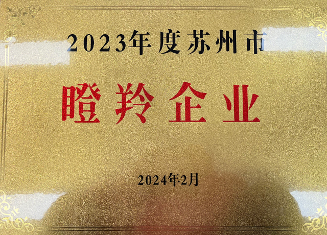
The company has a technical team of more than 90 members, led by doctors and senior industry experts, offering core intellectual support for technological breakthroughs. It has achieved fruitful R&D results, with a total of 24 invention patents, 42 utility model patents and 6 software copyrights applied for. These patented technologies have strengthened the core competitiveness of its products. With its comprehensive strength, the company has been awarded many honors including Suzhou Gazelle Enterprise and Jiangsu Province Specialized, Sophisticated, Unique and New Enterprise, establishing itself as an industry benchmark.
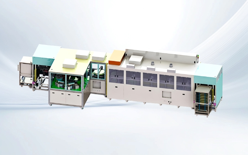
Its customers cover all segments of the semiconductor industry chain, including substrate manufacturers, FABs and national laboratories, serving more than 100 enterprises and winning wide trust. In October 2024, the company realized the overseas export of full-line equipment including lapping, polishing and cleaning machines. As of November 2025, a total of 568 sets of various semiconductor equipment had been delivered, marking remarkable achievements in its global layout. In the future, the company will uphold the philosophy of "Empowering the Industry with Technology", provide full-generational semiconductor material solutions, and support industrial innovation and independent control.
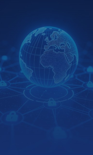

This is the core field, encompassing all devices that process and transmit information, such as computers, mobile phones, data centers, and communication networks.
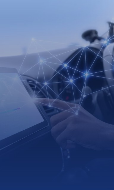

Covering electrification (power control), intelligence (autonomous driving chips), and connectivity (vehicle-to-everything), it is one of the fastest-growing fields.
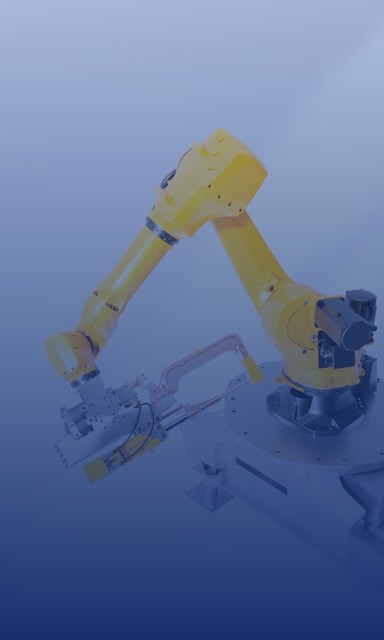

Driving industrial automation, robotics, smart grids, and renewable energy systems demands high reliability and high performance.


Used in high-end medical imaging equipment, vital signs monitoring, and portable diagnostic and therapeutic instruments, it is related to life and health.

Representing the future direction, it provides underlying hardware support for cutting-edge technologies such as massive smart devices, AI computing power explosion, and the metaverse.